

 العربية
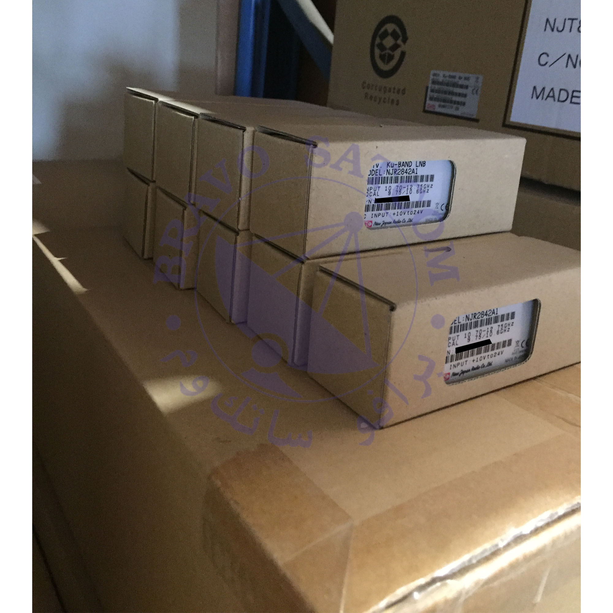

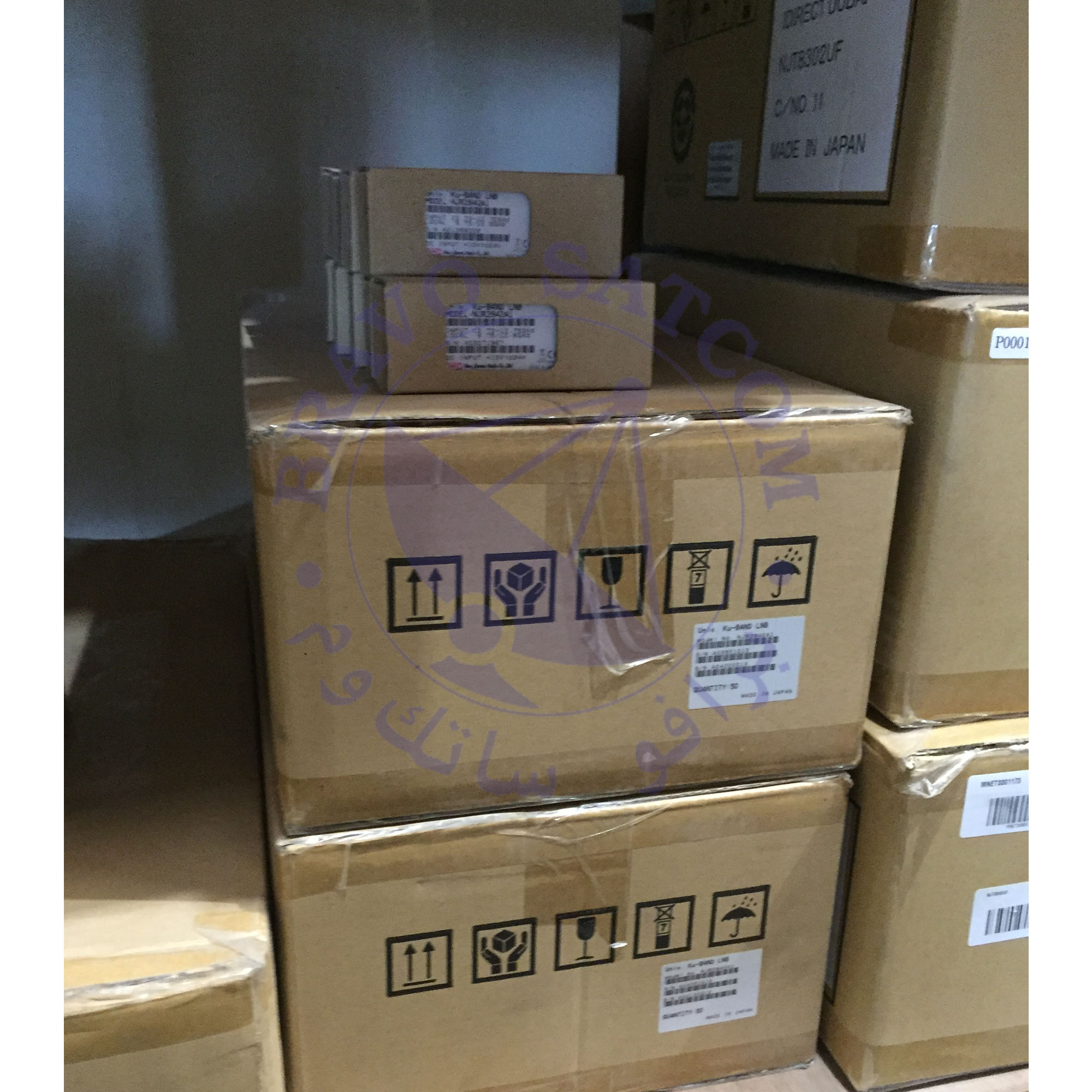
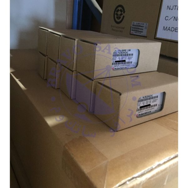
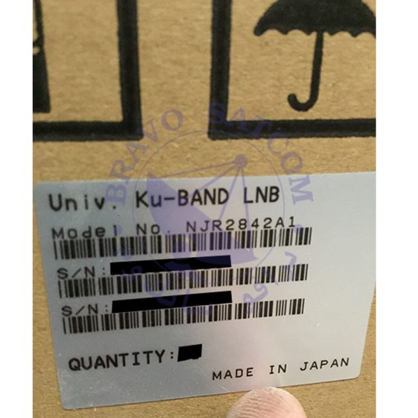
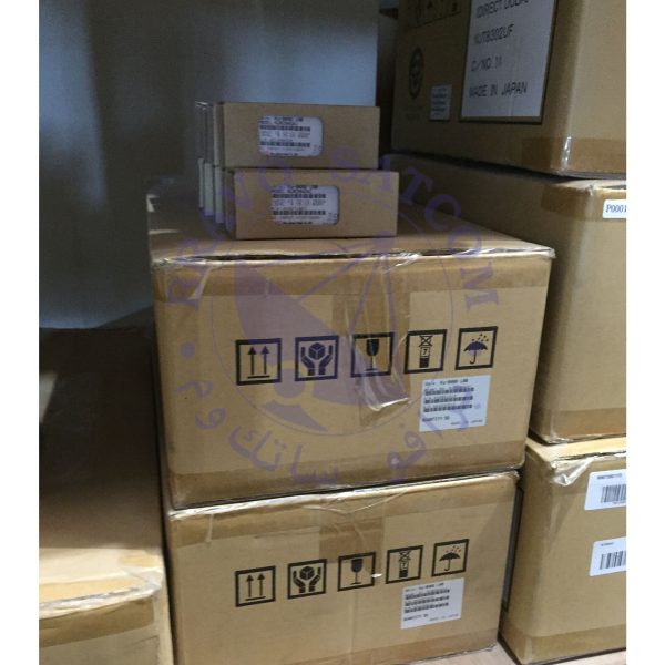
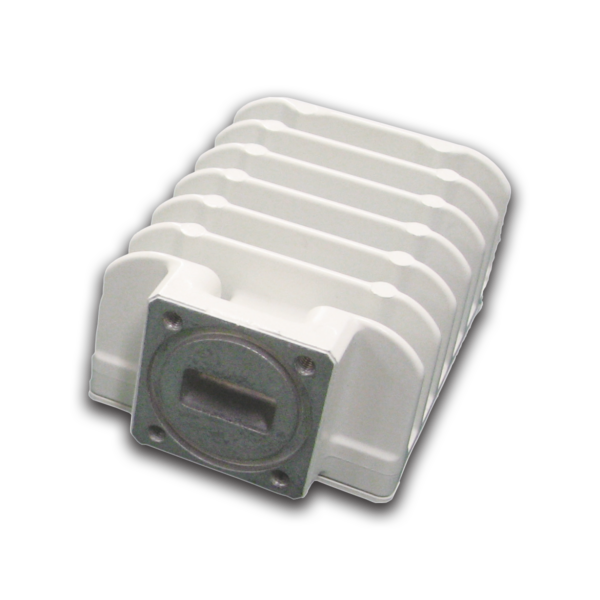
Universal Ku-band PLL LNB 10.7 to 12.75 GHz, NJR2842A1
- IF Output / DC Power Input: F-type Female Connector
- Band Select Function: 22 kHz Tone
- Input Frequency: (Low) 10.7 – 11.7 GHz / (High) 11.7 – 12.75 GHz
- Input Frequency Band Select: Outside Rotary Switch
- Internal Reference, Local Stability: +/-35 ppm
Frequency Bands
- Input Frequency Band
- Low Band: [10.70 – 11.70 GHz]
- High Band: [11.70 – 12.75 GHz]
- Output Frequency Band
- Low Band: [950 – 1,950 MHz]
- High Band: [1,100 – 2,150 MHz]
Local Frequency
- Low Band: 9.75 GHz
- High Band: 10.60 GHz
Performance Metrics
- Conversion Gain: 48 dB min., 62 dB max.
- Gain Variation:
- 6 dB max. over frequency
- 1.5 dB max. in any 36 MHz segment
- Noise Figure:
- at +25°C: 0.9 dB typ.
- over temperature: 1.1 dB typ.
Power Specifications
- Output Power for 1 dB Gain Compression: 0 dBm min. @ +25°C
- Output Intercept Point of 3rd Order Intermodulation: +5 dBm min.
Tx Signal Immunity
- Gain Change: 0.2 dB max.
- Noise Figure Change: 0.1 dB max.
- at -20 dBm Tx Input
Stability and Phase Noise
- Local Stability (Initial Setting Error & Over Temperature): +/- 35 ppm max.
- L. O. Phase Noise (SSB):
- @ 100 Hz: -50 dBc/Hz typ.
- @ 1 kHz: -70 dBc/Hz typ.
- @ 10 kHz: -75 dBc/Hz typ.
- @ 100 kHz: -85 dBc/Hz typ.
- @ 1 MHz: -105 dBc/Hz typ.
Phase Jitter and Leakage
- Integrate Phase Jitter (DSB): 2.5 deg RMS max. @ 100 Hz to 1 MHz
- Local Leakage Levels:
- at IF Output Connector: -40 dBm max.
- at RF Input Flange: -60 dBm max.
Image Rejection and Spurious
- Image Rejection: 40 dB min.
- Spurious:
- -120 dBm max. at input, fixed frequency spur, unrelated to test CW signal.
- -40 dBc typ., -30 dBc max. with test CW signal, -10 dBm IF output
Impedance
- Input V.S.W.R.: 2.5 : 1 typ.
- Output Impedance: 75 ohms nom.
- Output V.S.W.R.: 2.3 : 1 max.
Related products
Fast Selling